Xbox One GPU Memory Access: ONION, GARLIC, and more
This paper discusses aspects of the Xbox One GPU memory system from the perspective of the performance of a title running on the exclusive OS. Topics discussed include the ONION and GARLIC buses, ESRAM, the texture cache hierarchy, and how to avoid pitfalls in performance and correctness when sharing data between the CPU and GPU.
Memory access in Xbox One is complex. Many factors affect performance, often in an unintuitive way. To maximize bandwidth utilization and deliver the highest quality games, you must understand the effects that a title’s various actions can have on memory access performance.
Hardware overview
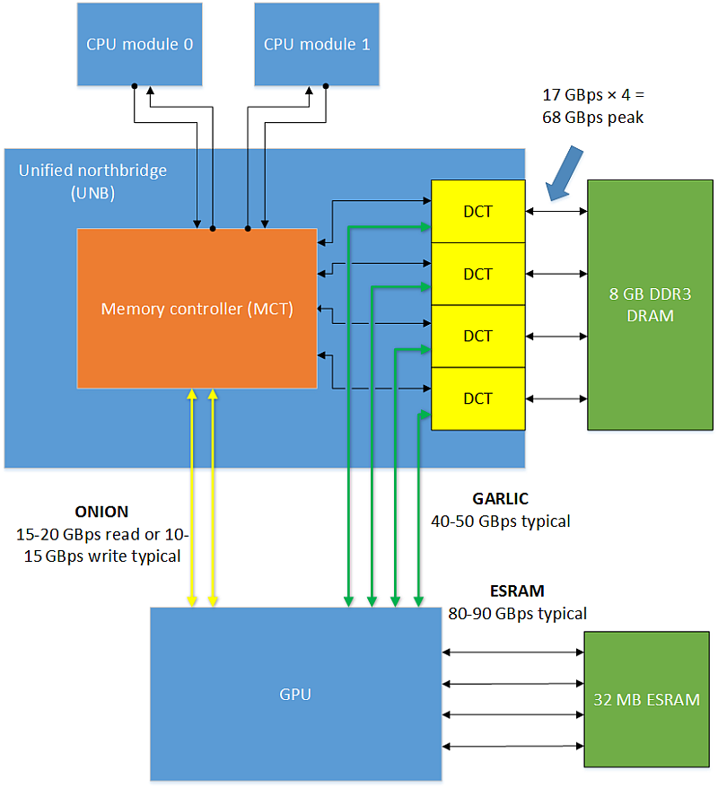
The Xbox One console contains 8 GB of unified DDR3 memory, 5 GB of which is accessible to exclusive OS titles. This memory is split into four channels that connect to four DRAM controllers (DCTs) in the unified Northbridge (UNB). Each channel provides 17 gigabytes per second (GBps) of peak bandwidth shared between reads and writes, for a total of 68 GBps of peak bandwidth between main memory and the UNB.
The two CPU modules connect to the DCTs via the memory controller (MCT). The MCT also provides memory access for other components of the system such as the Southbridge and the SHAPE audio processor.
Figure 1. Interaction between the Xbox One GPU and memory hardware
The Xbox One GPU can access main memory via two different buses:
- The graphics accelerated reduced latency integrated channel (GARLIC) bus is a four-channel bus capable of 68 GBps peak bandwidth (limited by the bandwidth of DRAM). Each of the four GARLIC channels is connected directly to one of the four DRAM controllers.
- The on-chip Northbridge to I/O noncoherent (ONION) bus is a two-channel bus capable of 24 GBps read or 15 GBps of peak write bandwidth, limited by components in the Northbridge. The two ONION channels connect to the MCT, which provides the ONION bus with some additional capabilities that GARLIC does not possess. Certain types of traffic must use the ONION bus.
Which bus is used for a particular memory transaction depends on the characteristics of the memory being accessed and the operation being performed.
Peak bandwidth is the amount of data that would be transferred per second if the bus were fully utilized—that is, transmitting useful data on every clock cycle. In practice this is unachievable. Various factors conspire to reduce the effective bandwidth available to the GPU, including contention from other consumers, bubbles introduced by request latency, and subtle interactions between various system components. In typical real-world rendering scenarios, you can expect to achieve around 40-50 GBps of combined read and write on the GARLIC bus and 15-20 GBps read or 10-15 GBps write-not at the same time-on the ONION bus.
The GPU memory controllers contain small FIFO write queues designed to prevent brief spikes in memory activity from stalling the rest of the pipeline. If these queues are full, the GPU is unable to issue additional memory operations. When traffic saturates the ONION bus for long periods of time, the write queues can fill up. In this situation, all GPU memory access, including access to GARLIC and ESRAM, can become limited by the bandwidth of the ONION bus.
ESRAM
Xbox One also contains 32 MB of high-speed ESRAM connected to the GPU via a dedicated bus. The ESRAM bus consists of four channels that run at 853 Mhz. In ordinary circumstances, each channel can transfer 32 B per clock cycle (read or write), leading to a theoretical bandwidth of:
4 channels × 32 B per clock × 853 Mhz = 109.2 GBps (using 1 GB = 109 B)
In some circumstances, the GPU can issue burst read requests to ESRAM. While a burst read is being fulfilled, the GPU can continue issuing write operations, effectively allowing reading and writing to occur in parallel. This can increase the achievable bandwidth past the 109.2 GBps maximum. The maximum sustained bandwidth that ATG has observed in experiments is approximately 133 GBps, with 80–90 GBps typical in standard rendering scenarios.
GPU texture caches
The GPU contains L1 and L2 texture caches which are used to mitigate the high latency of memory operations. The term texture cache is a bit of a misnomer; the texture caches are used for all memory accesses that are not handled by the color and depth blocks (CBs/DBs), most notably texture fetches, buffer reads, and unordered access view (UAV) reads and writes.
Figure 2. Xbox One texture cache hierarchy
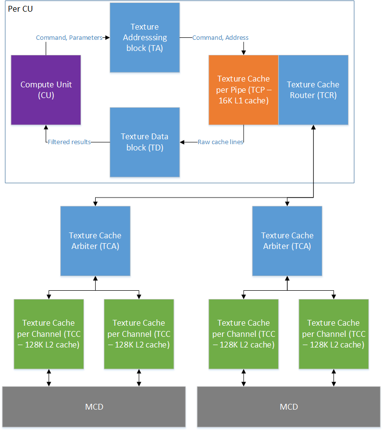
It is important to understand the components of the cache subsystem when you interpret memory-related performance counters in PIX. If a draw call or compute shader dispatch appears to be bound on memory access, yet the bus throughput is nowhere near peak, the bottleneck may lie somewhere in the cache hierarchy.
The diagram in Figure 2 shows the following components of the texture cache subsystem:
Texture Addressing Block (TA)
There is one TA per compute unit (CU). Each TA receives read and write requests from the CU and calculates the appropriate memory addresses to pass to the TCP. For writes, the TA converts values received from the CU into the target data format, and forwards the converted data to the TCP. It also coalesces memory requests (see “Coalesced accesses” later in this paper).
Texture Data Block (TD)
The TD receives raw memory from the TCP and, based on the selected data format, extracts values to pass to the CU. It also performs texture filtering.
Texture Cache per Pipe (TCP)
There is one TCP per CU. Each serves as a 16 KB L1 data cache for the CU. If a read request misses the TCP cache, the request is forwarded to the TCR.
Texture Cache Router (TCR)
There is one TCR per CU, and each is paired with a TCP. The TCR forwards requests from the attached TCP to the appropriate TCAs; it also forwards data from the TCAs back to the TCP.
Texture Cache Arbiter (TCA)
The TCA manages the request and data streams for a pair of TCCs. It also buffers requests from the TCRs and routes each request to the appropriate TCC.
Texture Cache per Channel (TCC)
There are four TCC total; each TCC is roughly correlated with one of the four memory channels. Each TCC contains 128 KB of cache memory, totaling 512 KB of L2 cache. Requests that miss the TCC cache are forwarded to the appropriate MCD.
Memory Controller, Data (MCD)
The MCD manages a pair of memory channels, routing ESRAM and main memory requests to the appropriate bus.
Coalesced accesses
For a given SIMD, the TA/TCP can process four fetches per cycle of up to 128 bits (16 bytes) each, for a total of 512 bits (64 bytes) fetched per cycle. This means a memory-read instruction normally takes 16 clock cycles (64 threads ÷ 4 threads per clock) to issue across an entire wavefront.
If a read instruction requests fewer than 128 bits from memory, some portion of the 512-bit data return bus will go unused. For example, if each thread in a wavefront requests a single floating point value (32 bits) from a texture or buffer resource, only 128 bits total (4 requests × 32 bits) will be fetched each cycle. This is only one quarter of the maximum possible throughput.
When reading single-component values from a texture in HLSL, the Gather methods can be used to fetch four values at a time, improving utilization of the data return bus. However, Gather is not supported for buffer resources. Instead, when reading from a buffer resource, if adjacent threads access adjacent memory locations, the TA can, under some circumstances, coalesce the requests. A common situation where reads can be coalesced is if all 16 threads in a quarter-wavefront access a contiguous, cache-line aligned range of 32-bit elements from a UAV or structured buffer. This allows all 16 fetches to issue in a single cycle, coalesced into four contiguous 128-bit reads. In general, to achieve coalescing, prefer structure-of-arrays (SoA) buffer layouts to array-of-structures (AoS) layouts.
Example
In the following example, a simple compute shader dispatch call is analyzed by using PIX performance counters to track down a bottleneck related to the cache subsystem.
| Name | Analysis ?? | VALUBusy(% ?? | WaitingVMCounter(% ?? | WaitingVMEM(% ?? | TexUnitBusy(% ?? |
|---|---|---|---|---|---|
| IT_DISPATCH_DIRECT | 89,500 | 1,278 | 3,792 | 44.636 | 97.079 |
This dispatch call spends about 45% of its time waiting to issue vector memory instructions, and the texture unit is busy nearly 100% of the time.
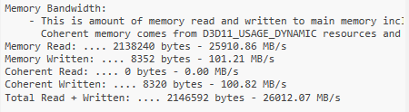
The Memory Bandwidth statistics in Dr. PIX reveal that all memory traffic for this dispatch occurs over the GARLIC bus. However, the dispatch still only achieves an effective throughput of 26 GBps, or about 50% bus utilization. This means the bus is likely not a bottleneck.
| GBRM_PERF_SEL_GUI_ACTIVE | TA_PERF_SEL_TA_BUSY | TCP_PERF_SEL_TCP_TA_ADDR_STALL_CYCLES |
|---|---|---|
| 60,360 | 58,910 | 56,086 |
The GBRM_PERF_SEL_GUI_ACTIVE counter gives the number of cycles when the GPU was active, while TA_PERF_SEL_TA_BUSY gives the number of cycles when the TA was busy. TCP_PERF_SEL_TCP_TA_ADDR_STALL_CYCLES gives the number of cycles when the TA was stalled by the TCP. In this case, the TA was stalled for almost the entire duration of the dispatch.
| TCP_PERF_SEL_TCR_TCP_STALL_CYCLES |
|---|
| 145 |
TCP_PERF_SEL_TCR_TCP_STALL_CYCLES gives the number of cycles when the TCP was stalled by the TCR. If the dispatch were bottlenecked by the L2 cache or by the memory bus, this number should be large relative to TCP_PERF_SEL_TCP_TA_ADDR_STALL_CYCLES. Since this number is small, the stall most likely occurs inside the TCP.
| TCP_PERF_SEL_READCONFLICT_STALL_CYCLES | TCP_PERF_SEL_READ_TAGCONFICT_STALL_CYCLES |
|---|---|
| 33,024 | 33,024 |
Upon closer examination of the other TCP counters, the numbers from TCP_PERF_SEL_READCONFLICT_STALL_CYCLES and TCP_PERF_SEL_READ_TAGCONFICT_STALL_CYCLES were found to be fairly large. It is apparent from the descriptions for these counters that read operations are being stalled due to contention for limited resources inside the TCP.
| TA_PERF_SEL_BUFFER_COALESCED | TA_PERF_SEL_BUFFER_TOTAL_CYCLES |
|---|---|
| 0 | 11,088 |
Finally, comparing TA_PERF_SEL_BUFFER_COALESCED to TA_PERF_SEL_BUFFER_TOTAL_CYCLES shows that no read operations are being coalesced.
Following is the shader code for the preceding dispatch call:
  struct BufferElement
  {
      float data[16]; // 16 floats = 64 bytes = one cache line
  };

  StructuredBuffer<BufferElement> g_Buffer   : register(b0);
  RWStructuredBuffer<BufferElement> g_RWDummyBuffer   : register(b1);

  [numthreads(64, 1, 1)]
  void CS( uint3 DispatchThreadID    : SV_DispatchThreadID )
  {
      uint thread = DispatchThreadID.x;

      float n = 0;
      for( int i = 0; i < 16; ++i )
      {
          n += g_Buffer[ thread ].data[ i ];
      }

      // Force compiler to retain the calculation, but don't do anything with it
      if( n == 12345678 )
      {
          g_RWDummyBuffer[ thread ].data[ 0 ] = n;
      }
  }
This example is a bit contrived, but you can see that this shader reads 16 floating point values from a structured buffer. Each thread reads from a separate cache line, which means the TA is not able to coalesce reads.
To facilitate read coalescing, the buffer data layout can be rearranged as follows. Note the modified portions of the code:
  struct BufferElement
  {
      float data;
  };

  StructuredBuffer<BufferElement> g_Buffer[16];
  RWStructuredBuffer<BufferElement> g_RWDummyBuffer   : register(b1);

  [numthreads(64, 1, 1)]
  void CS( uint3 DispatchThreadID    : SV_DispatchThreadID )
  {
      uint thread = DispatchThreadID.x;

      float n = 0;
      for( int i = 0; i < 16; ++i )
      {
          n += g_Buffer[i][ thread ].data;
      }

      // Force compiler to retain all the calculation, but don't do anything with it
      if( n.x == 12345678 )
      {
          g_RWDummyBuffer[ thread ].data = n;
      }
  }
With this data layout, the 16 threads in a quarter-wavefront will read contiguous values from the same cache line. This provides the following results.
| TA_PERF_SEL_BUFFER_COALESCED_READ_CYCLES | TA_PERF_SEL_BUFFER_TOTAL_CYCLES |
|---|---|
| 2,752 | 2,752 |
The TA_PERF_SEL_BUFFER_COALESCED_READ_CYCLES counter indicates that reads are being coalesced.
| Name | Analysis ? | GRBM_PERF_SEL_GUI_ACTIVE | TexUnitBusy (% ?? |
|---|---|---|---|
| IT_DISPATCH_DIRECT | 41,660 | 43,176 | 77,561 |
The total GPU time drops significantly, as does the texture unit utilization.
| TCP_PERF_SEL_READCONFLICT_STALL_CYCLES | TCP_PERF_SEL_READ_TAGCONFLICT_STALL_CYCLES | TCP_PERF_SEL_TCR_TCP_STALL_CYCLES |
|---|---|---|
| 0 | 0 | 29,166 |
The stalls previously encountered inside the TCP disappear; the TCP becomes bottlenecked by the TCC and/or memory bus.
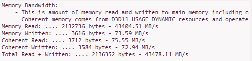
And although the same amount of data is read from main memory, the effective throughput of the bus increases to 43 GBps, which is much closer to the maximum achievable bandwidth.
Memory coherence and access flags
The CPU and GPU both contain write-back caches designed to reduce the performance impact of main memory accesses. When data is shared between the CPU and GPU, take care to ensure that neither reads stale data from cache. Memory traffic generated by the GPU can be either noncoherent or I/O-coherent, depending on the page descriptor flags for the memory being accessed.
Noncoherent traffic essentially behaves as if the CPU did not exist. It can typically use the faster GARLIC bus, with the following results:
GPU Reads
If a given memory location is present in one of the GPU caches, a GPU read from that memory location returns the cached value. The GPU fetches cache lines directly from DRAM. The GPU does not examine the CPU caches.
GPU Writes
When a modified cache line is evicted from the GPU’s L2 cache, the cache line is written directly to DRAM. The CPU caches may contain stale values.
I/O-coherent traffic snoops the CPU caches via the MCT in the Northbridge. I/O-coherent traffic can be a performance bottleneck, because it must use the slower ONION bus, with the following results:
GPU Reads
When fetching a cache line from main memory, the GPU first probes the CPU caches. If the given memory location is not present in the CPU caches, the GPU fetches the value from DRAM.
GPU Writes
When a modified cache line is evicted from the GPUÆs L2 cache, the GPU probes the CPU caches and invalidates any entries that refer to the modified location. The GPU then writes the modified cache line to DRAM.
I/O coherence allows you to avoid costly flushes of the CPU cache after writing to a resource on the CPU. This makes I/O coherence useful for small, frequently updated resources, such as constant buffers. However, as described in Xbox One Memory System, I/O coherence works only one way: the GPU snoops the CPU caches, but not vice versa. This means the GPU caches still need to be flushed if the resource is modified by either the CPU or the GPU.
When allocating main memory via D3DAllocateGraphicsMemory, you can choose from one of three memory types:
Cached Noncoherent
- D3D11_GRAPHICS_MEMORY_ACCESS_CPU_CACHE_NONCOHERENT
- Memory is cached by both the CPU and the GPU.
- GPU memory access is noncoherent, and it can usually use the GARLIC bus.
- If memory is written by the CPU, the appropriate ranges in both the CPU and GPU caches must be flushed before reading on the GPU.
- Cached noncoherent memory is not recommended for scenarios involving GPU writes and CPU reads, because this is dangerous and difficult to perform correctly.
Cached Coherent
- D3D11_GRAPHICS_MEMORY_ACCESS_CPU_CACHE_COHERENT
- Memory is cached by both the CPU and the GPU.
- GPU memory access is I/O coherent, and it always uses the ONION bus.
- If memory is written by the GPU, the appropriate range in the GPU caches must be flushed before reading on the CPU.
- If memory is written by the CPU, the appropriate range in the GPU caches must be flushed before reading on the GPU.
Write Combined Noncoherent
- D3D11_GRAPHICS_MEMORY_ACCESS_CPU_WRITECOMBINE_NONCOHERENT
- Memory pages are cached by the GPU, but not by the CPU.
- CPU writes are write combined.
- GPU memory access is noncoherent, and can usually use the GARLIC bus.
If memory is written by the CPU, the write combine buffers must be flushed (via a write memory barrier), and the appropriate range in the GPU caches must be flushed before accessing on the GPU.
The CPU caches can be flushed by using D3DFlushCpuCache. The GPU caches can be flushed by using ID3DXboxPerformanceContext::FlushGpuCaches or ID3DXboxPerformanceContext::FlushGpuCacheRange. The Xbox One driver does not automatically flush the CPU or GPU caches on a call to Map or Unmap.
Default usage resources
Placement set functions such as CSSetPlacementConstantBuffer can be used to quickly and safely update a DEFAULT resource while simultaneously binding it to the rendering pipeline. We strongly recommend that titles use the placement set functions for resource updates whenever possible. However, for ease in porting of existing Direct3D 11 engines, it is also possible to update DEFAULT resources using Map and Unmap.
When you map a DEFAULT usage resource, you must pass the D3D11_MAP_FLAG_ALLOW_USAGE_DEFAULT flag:
  D3D11_MAPPED_SUBRESOURCE MapData = {};
  m_pd3dContext->Map(pCurrentCBVertex, 0, D3D11_MAP_WRITE_NO_OVERWRITE, D3D11_MAP_FLAG_ALLOW_USAGE_DEFAULT, &MapData);
Also note the map type. The allowed map types for DEFAULT usage resources on the immediate context are:
- MAP_READ
- MAP_WRITE
- MAP_READWRITE
- MAP_WRITE_NO_OVERWRITE
Deferred contexts support only MAP_WRITE_NO_OVERWRITE, which is implemented as MAP_WRITE, but without checking for CPU-GPU synchronization. So, use this map type with caution.
The other three map types perform proper synchronization checks before returning the CPU memory pointer. This synchronization can result in a CPU stall if the resource is still in use by the GPU. In order to prevent such stalls, titles should double-buffer resources that are frequently updated.
In the July and August XDKs, the driver allocates DEFAULT usage resources in cached noncoherent memory. In a future XDK release the default memory type will be changed to write combined noncoherent. If you wish to override the default memory type, you can use the placement resource creation APIs to create resources in memory previously allocated via D3DAllocateGraphicsMemory.
Memory encryption and partial writes
Title memory on Xbox One can optionally be encrypted in DRAM. The DCTs perform encryption and decryption at a 16-byte (128-bit) granularity. For this reason, read and write requests to the DCTs for encrypted memory must be a multiple of 16 bytes.
Partial writes (that is, writes smaller than 16 bytes) require a read-modify-write operation: the 16-byte block that contains the target must be fetched from the appropriate DCT, modified, and sent back to the DCT to be written to DRAM. Read-modify-write operations consume a larger amount of DRAM bandwidth than standard read or write operations. Additionally, GPU does not have the ability to perform read-modify-write operations via the GARLIC bus, so partial writes to encrypted memory are forced to use the slower ONION bus.
Though encryption is performed on 16-byte blocks, the memory interface between the GPU and the ONION and GARLIC buses is 32 bytes wide. Therefore, when there is a partial modification to either the first or second word of a 32-byte chunk, the entire 32-byte transaction will be routed over ONION.
Partial writes can be caused by many things, including but not limited to:
- Masked writes to resourcesùfor example, by performing a draw with the RenderTargetWriteMask member of the D3D11_RENDER_TARGET_BLEND_DESC Structure set to something other than D3D11_COLOR_WRITE_ENABLE_ALL.
- Small, scattered writes to a UAV in a compute shader.
- Rasterization of primitives with low quad efficiency, including points, lines, and small triangles.
- Spilling of internal GPU data structures to memory.
To aid in avoiding performance penalties caused by partial writes to encrypted memory, titles can specify which pages should be encrypted. Any page not mapped with MEM_GRAPHICS will be encrypted. Pages mapped with MEM_GRAPHICS will be encrypted if one or more of the following flags are specified for the page: PAGE_GPU_READONLY, PAGE_GPU_COHERENT, or PAGE_GPU_EXECUTE. Otherwise, a page will be stored unencrypted. The XMemAlloc memory types for graphics allocations correspond to the combinations of page protection flags shown in the following table.
XMemAlloc memory types
| Memory type | Protection flags |
|---|---|
| XALLOC_MEMTYPE_GRAPHICS_WRITECOMBINE | 0 |
| XALLOC_MEMTYPE_GRAPHICS_WRITECOMBINE_GPU_READONLY | PAGE_GPU_READONLY |
| XALLOC_MEMTYPE_GRAPHICS_CACHEABLE | PAGE_GPU_COHERENT |
| XALLOC_MEMTYPE_GRAPHICS_CACHEABLE_NONCOHERENT | 0 |
| XALLOC_MEMTYPE_GRAPHICS_COMMAND_BUFFER_WRITECOMBINE | PAGE_GPU_EXECUTE |PAGE_GPU_READONLY |
| XALLOC_MEMTYPE_GRAPHICS_COMMAND_BUFFER_CACHEABLE | PAGE_GPU_EXECUTE |PAGE_GPU_READONLY |PAGE_GPU_COHERENT |
Hub transactions
The GPU contains four render backends (RBs) that receive the final color and depth information for a draw event. A pixel is assigned to an RB based on screen-space position: the screen is divided into a checkerboard pattern of 32×32 pixel supertiles, and adjacent supertiles are assigned to different shader engines. Within a supertile, each sub-block of 8×8 pixels corresponds to a different RB.
Each RB connects to one of the four GARLIC channels. A render target created using a 2D tiling mode (such as XG_TILE_MODE_2D_THIN) can write its pixel data directly to DRAM via the connected GARLIC channel. However, if the render target is created using a 1D or linear tiling mode, then some pixels may need to be rerouted to a different memory channel—which means the pixel data must be sent through the graphics memory controller hub. The pixel data will still travel to DRAM via the GARLIC bus, but having to pass through the hub significantly reduces RB throughput. To avoid this performance penalty, always use a 2D tiling mode for your render targets.
Also minimize writes to the backbuffer. The display controller requires a special tiling mode for backbuffer textures, which causes backbuffer writes to incur a high number of hub transactions.
Profiling memory traffic in PIX
PIX has several resources available for profiling memory traffic.
On the Dr. PIX tab, the Memory Bandwidth section displays the total amount of memory traffic generated by a particular draw call or by the entire scene. Dr. PIX also displays the amount of coherent memory traffic. The following example shows the details that the Memory Bandwidth section displays:
  Memory Bandwidth:
      - This is amount of memory read and written to main memory
      including coherent memory.
        Coherent memory comes from D3D11_USAGE_DYNAMIC resources and
        operates at 1/2 rate read and 1/4 rate write.
  Memory Read: .... 154830272 bytes - 7044.27 MB/s
  Memory Written: .... 143616 bytes - 6.53 MB/s
  Coherent Read: .... 14682816 bytes - 668.02 MB/s
  Coherent Written: .... 143616 bytes - 6.53 MB/s
  Total Read + Written: .... 154973888 bytes - 7050.80 MB/s
These statistics are based on OnionReadMem, OnionWriteMem, GarlicReadMem, and GarlicWriteMem, which are derived counters available on the Counters tab in the Memory related section. The bandwidth numbers are calculated by dividing the amount of memory transferred by the total time taken for the draw call. If you see low numbers for bandwidth, they do not necessarily mean that there is a problem; it may simply mean the draw is not bound by bandwidth.
Also on the Dr. PIX tab, the HUB remote transactions section displays the number of reads and writes that had to pass through the graphics memory controller hub. The following example shows the details that the HUB remote transactions section displays:
  HUB remote transactions
  HUB pre-translated transactions are very high latency memory transactions
  that occur when CB or DB accesses memory in inefficient pattern.
  This happens for example when you use linear tiling for your render targets.
  Each transaction can be 32 to 256 bytes in size so the number of bytes read
  may be variable.
    206900 reads, 519594 writes.
These statistics are based on HUBRead and HUBWrite, which are derived counters available on the Counters tab in the Memory related section.
The PIX Resources tab describes the memory attributes of each resource bound during a draw call-including the size, the address, the tiling mode, whether the resource memory is cached or uncached, and whether the resource memory is coherent or noncoherent.