How Do VMEM Instructions Work?
This topic explains the vector memory class of shader instructions. A solid understanding of how VMEM instructions work is important for making the right decisions during the shader optimization process. The topic is intended for graphics programmers and assumes certain familiarity with the Xbox One GPU and DirectX. Please see the documents listed in the references section for a recap.
Vector memory instructions transfer one or more pieces of data uniquely for each shader thread of a wavefront. In the Xbox One GPU, they are used in all types of shaders to read vertex data, texture data, and dynamically indexed constant buffer data; to read and write unordered access views; and to perform atomic operations. While the performance of ALU instructions is predictable, performance of vector memory instructions is more complex and requires an understanding of how multiple modules work inside the GPU. With the information contained in this topic, you should be able to analyze the shader assembler code in PIX and apply memory optimizations to your shaders.
Glossary
The following abbreviations and acronyms are used in this topic.
| CU | Compute unit |
|---|---|
| VALU | Vector ALU instruction |
| SALU | Scalar ALU instruction |
| VMEM | Vector memory instruction |
| SMEM | Scalar memory instruction |
| SQ | Sequencer |
| SGPR | Scalar GPR |
| VGPR | Vector GPR |
| TA | Texture addressing |
| TCP | Texture cache per pipe (L1 cache) |
| TCC | Texture cache per channel (L2 cache) |
| TD | Texture data |
| LDS | Local data store |
| EXP | Shader export instruction |
| Wave | Wavefront is one unit of work comprising 64 shader threads |
| GLC | Globally coherent |
| GDS | Global data store |
| UAV | Unordered access view |
Buffer instructions and image instructions
Buffer instructions are generated for reads, write, or atomic operations on vertex buffers, raw buffers, or structured buffers. No data filtering or samplers are supported. Data is transferred via the L1 and L2 caches both for reads and writes. There are two kinds of buffer instructions:
tbuffer_*
Typed buffer instruction. Data format is specified in the instruction and atomics aren’t supported.
buffer_*
Untyped buffer instruction. Data format is specified in the buffer object descriptor. Optional format conversion can be specified as part of the instructions. Atomics are supported.
Image instructions are generated for reads, writes, or atomic operations on texture maps and typed surfaces. Filtering is supported for reading data. Data is transferred via the L1 and the L2 caches both for reads and writes. All image instructions have a data mask field that specifies which channels it receives. There are two kinds of image instructions:
sample_*
Read and filter data from a texture. These operations require a sampler.
image_*
Read, write, or perform an atomic operation on a texture. No filtering is supported.
There are more types of vector memory instructions, but they are relatively rare and are not covered in this topic.
Cheat sheet: summary performance table
These are peak performance numbers.
| Minimal cost in the shaders | |
|---|---|
| Buffer single-channel read | 4 clocks |
| Buffer multichannel read | 16 clocks |
| Buffer atomic | 16 clocks |
| Texture point-sampled fetch | 16 clocks any format |
| Bilinear texture fetch | 16 clocks ≤ 32bpp, 32 clocks 64bpp, 64 clocks 128bpp |
| Trilinear texture fetch | Bilinear texture fetch × 2 |
| Anisotropic xN texture fetch | (Cost of a bilinear texture fetch or of a trilinear texture fetch) × N |
| Peak speed across the entire GPU | |
|---|---|
| Buffer single-channel read | 192 32bpp values per clock with coalescing |
| Texture read | 48 per clock |
| Peak speed in seconds | |
|---|---|
| Reading or writing a 1080p 32bpp texture | 50 μs |
These are rarely achievable in practice, but they are useful to remember for a quick analysis of a shader. Here are some quick rules of thumb that can be inferred from the performance table.
- Any texture fetch costs at least 16 clocks. Make it count by reading as much data as you can. Gather4 is a valuable tool when working with single-channel textures.
- Sometimes it’s cheaper to read one U32 value from a buffer using single-channel read and decompress it on the ALU than to read 2–4 distinct byte values by using a multichannel read.
It’s impossible to list the performance of vector memory instructions for a general case. Real-life latency of texture instructions is variable and often greater than 100 clock cycles; sometimes it is in the range of 400 clock cycles when there is a cache miss.
Latency hiding
Due to high latency of vector memory instructions, the GPU uses two latency hiding mechanisms.
Vector memory instructions are designed to not block wavefront execution at the point where they are issued. Each issued vector memory instruction increments a VM counter and each returned vector memory instruction decrements the counter. The shader compiler implements manual synchronization by inserting s_waitcnt instructions before the point where the results are needed; otherwise, results are undefined. Vector memory instructions always return in order. An example of this shown in the following table.
| image_sample v[2:5], v[2:5], s[4:11], s[0:3] dmask:0xf | Instruction issue starts. VM counter is incremented. |
|---|---|
| v_interp_p1_f32 v6, v0, attr2.wv_interp_p1_f32 v7, v0, attr2.zv_interp_p2_f32 v6, v1, attr2.wv_interp_p1_f32 v8, v0, attr2.yv_interp_p2_f32 v7, v1, attr2.z | Instruction issue ends.Wave continues executing instructions without blocking, essentially reducing memory latency. Shader compiler works really hard to put work here. |
| s_waitcnt vmcnt(0) | Here is when the latency is seen. If the memory instruction hasn’t returned yet, the VM counter is still 1, and the wave is put into waiting mode. |
If a wave is in wait mode, it can’t continue execution while the VM counter is greater than the value specified in the s_waitcnt’s parameter. In this case, latency is hidden by running other waves that exist on the same SIMD. The more waves are available, the better latency hiding works. The number of waves per SIMD is called occupancy and is something developers should strive to maximize. Measured occupancy can be seen in the Dr. PIX topic’s ALU and Performance sections and also using column counters.
Note The same mechanism is applied to LDS, SMEM, and EXP/GDS instructions. However, they use different counters.
Hardware-level overview of a texture unit
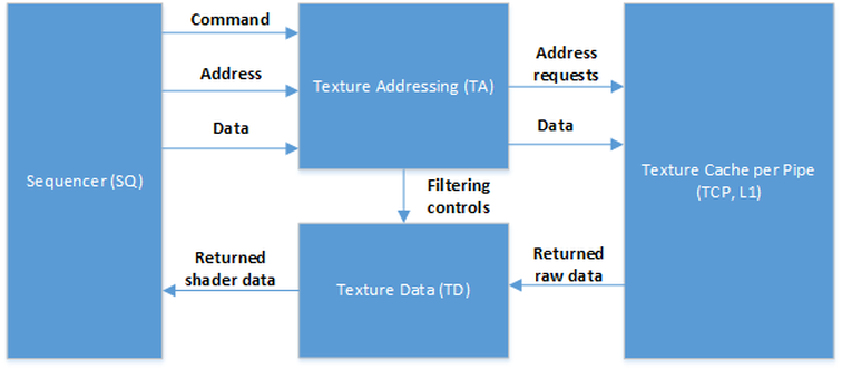
Here is a schematic overview of the texture unit inside of a compute unit. L2 cache and memory aren’t shown.
Figure 1. Top-level overview of the TA/TCP/TD
In the life of a vector memory instruction
The cost of each VMEM instruction comprises issue time (SQ–>TA), memory request issue time (TA–>TCP), memory read time (TCP->TD), and data return time (TD–>SQ). It is possible to be bound on any of those four stages, although most commonly games are bound on memory access.
Stage 1: Instruction issue
Each of the 12 CUs supports up to 40 waves. They are split into four groups of up to 10 waves (one group per SIMD), and during each cycle one SIMD is chosen for processing. The four cycles that a CU takes to go around the four SIMDs is called a phase or a wait-cycle. During each clock cycle, all 10 waves compete to issue one instruction of each type: VALU, SALU, VMEM, LDS, EXP/GDS, and Branch. For more information, see the Xbox OneGPU Shader Cores white paper, available for download from the Xbox Game Developer (XGD) site.
VMEM instructions use a single TA bus which is shared by all four SIMDs. Even though each SIMD can choose to issue a VMEM instruction every clock cycle, the quickest it can issue one is one every four clocks.
In order to issue a VMEM instruction, the operands in SGPRs and VGPRs need to be transferred to the TA. Until all operands of the instruction are transferred to the TA, the issuing wavefront can’t go to the next instruction, and no other wave on the CU can use the TA bus. The shortest VMEM instruction issue takes four clocks, therefore the issue rate limit. VMEM instruction, like some other types of instructions, essentially serializes wavefronts across all four SIMDs.
Depending on how much data needs to be sent, a VMEM instruction issue takes a variable number of clock cycles. This makes sense because there can be as many as 64 different UV coordinates, offsets, gradients, and other pieces of data per instruction. So it can’t be made instantaneous.
The operands for the VMEM instruction are split into three streams and sent over three parallel busses: Command, Address, and Data. Instruction issue speed is governed by the longest time among those three busses. The following table provides a few examples of how long it takes to issue a VMEM instruction for a wavefront based on the number and size of the operands.
| Command, clk | Address,clk | Data,clk | Total, clk | |
|---|---|---|---|---|
| Image1D read, 128bit descriptor | 8 (4 texture + 4 sampler) | 4, 1D coord | 0, no data | 8 |
| Image2D read, 256bit descriptor | 12 (8 texture + 4 sampler) | 8, 2D coord | 0, no data | 12 |
| Buffer read | 4 (buffer) | 4, 1D coord | 0, no data | 4 |
| Buffer single channel write | 4 (buffer) | 4, 1D coord | 4, 1 DWORD | 4 |
| Image2D write | 8 (texture) | 8, 2D coord | 16, 4 DWORDs | 16 |
On large workloads, it is only possible to be bound on VMEM instruction issue itself if issue time is greater than 16 clock cycles. Otherwise, the TA will usually be the bottleneck. For example, SampleGrad() with 2D texture will cost 24 cycles to issue and will be approximately two times more expensive than a regular Sample() (12 clock cycles) if all reads hit the L1 cache.
In the case of SampleGrad(), we can see in Dr.PIX these telltale signs of being issue bound.
Waiting to issue VMEM 80.91, %
VALU                                         259
  Cost per inst                            1, clks
VMEM_RD                                    16
   Cost per inst                           5.999, clks
Based on this data, the shader is VMEM issue bound. The number of cycles that it takes to process VMEM is 384 (16 × 5.99 × 4), which is greater than number of cycles VALU takes (259).
After the VMEM instruction is issued, the wavefront can continue. The instruction itself now continues execution inside the TA block.
Stage 2: Computing addresses and requesting data
The TA continues execution of the VMEM instruction by requesting the data from the TCP and informing the TD about what return data to expect and how to filter it. The TA can request up to 128 bits of data from four locations per clock. Peak read speed of the TCP matches that. This enables peak bilinear rate of 2×2 filtered pixels per clock at less than or equal to 32bpp or an unfiltered rate of 4 pixels per clock at up to 128bpp.
Figure 2. Outline of the bilinear filtered texture fetch process. This process is repeated for all quads in the wavefront.

One VMEM instruction can trigger more than one memory request, so a VMEM instruction retires from TA only after all its requests are sent. Here is where the extra cost for trilinear and anisotropic filtering is first seen, for example. The TA needs to request all samples from the TCP for a requested texel, and some fetches will have to be run over many clock cycles.
The following table shows the peak speeds in the TA. This table shows how long it takes the TA to send data requests to the TCP.
| Speed | Comment | |
|---|---|---|
| Point sample fetches | 4 pixels/clk (16 clocks/wave) | Any format |
| Bilinear fetches, ≤ 32bpp | 4 pixels/clk (16 clocks/wave) | ≤32 bit per pixel full speed |
| Trilinear fetches, ≤ 32bpp | Bilinear / 2 | GPU will try to optimize this to bilinear when it can. |
| Anisotropic Nx, ≤ 32bpp | (Bilinear or Trilinear) / N | Tri-juicing is also available.* |
| Bilinear, Trilinear, Aniso 64bpp | 32bpp rate / 2 | |
| Bilinear, Trilinear, Aniso 128bpp | 32bpp rate / 4 | |
| Buffer single-channel load | 16 threads / clk (4 clocks/wave) | With coalescing, 4 threads/clk without coalescing. |
| Buffer multi-channel load | 4 threads / clk (16 clocks/wave) | |
| Buffer atomics | 4 threads / clk (16 clocks/wave) |
* See the PerfMip field of the D3D11X_SAMPLER_DESC Structure
Here are some extra costs that need to be paid for the following features (per 2×2 quad).
- Border color adds one or two cycles.
- Custom gradients will add up to three clocks.
- Cubemap corners may add up to five clocks.
- Non pow-2 wrap cases may add up to three clocks.
It is possible to get a severe bottleneck here due to this accumulated cost as this cost can theoretically run into thousands of cycles per wavefront. Anisotropic filtering is the prime example where this cost can dominate shader execution.
To detect bottlenecks due to anisotropy, use this Dr. PIX counter: Measured duration with anisotropic filtering turned off: 1715040 ns (54% faster)
If this is a high number, set PerfMip to enable tri-juicing optimization of trilinear or trilinear anisotropic filtering in this case. It will enable switching to bilinear filtering in cases where texture LOD is near an integer.
TA block also performs coalescing of single-channel read, write, and atomic requests to buffers. When a single-channel buffer fetch is used with less than or equal to 32bpp formats, much of the TCP-to-TD bandwidth may end up unused. To make use of that bandwidth, the TA is designed so that if it detects that consecutive shader threads request addresses can be read in the same 128-bit request, it coalesces the reads and can return up to 16 elements per cycle for single-channeled 8, 16, and 32bpp formats. This enables faster single-channel buffer reads, but only if TA can coalesce reads from four blocks of four threads at a time.
Figure 3. Coalescable case. Data for four blocks of four threads can be read from four memory locations.

Figure 4. Non-coalescable case. None of four locations can be coalesced.

TA also processes Gather4 instruction. Gather4 allows the TD to return unfiltered single-channel data from each of the 16 texels per clock. It is the same speed per DWORD as a single-channel coalesced buffer read. Take, for example, a Gather4 of an R32 texture. It can return 4 DWORDs of data per thread in 16 clocks. A regular point-sampled image fetch returns 1 DWORD of data per thread in 16 clocks, which is four times less data per clock. A point-sampled fetch would be able to read one 4×32 value per thread if R32G32B32A32 was aliased on top of an R32 texture, but in general it’s not possible due to different tiling modes between 128bpp and 32bpp texture formats.
Stage 3: TCP loads the data and passes it to the TD
The TCP is the “L1” cache. The TCP is per CU, it is 16 KB in size, has four interleaved RAMs, each fully associative with 64 tags and LRU policy. The TCP stores raw memory bytes. It deals with reading and writing image and buffer data, write-combining for write and atomic requests, read-combining for read requests, handles memory tiling and block format decompression on read, and also handles partially resident textures. The point of the TCP is to hide latency of the TCC, not to store data there for a long time.
At peak rate, the TA can request four unique addresses per clock, and the TCP can return up to 128 bits of data from each address to the TD per clock. It’s guaranteed that the TCP can send to TD any 2×2 image texel in 1 clock.
Real life performance is governed by the size of the request and scattering in memory. For each L1 cache miss, a request is forwarded to the L2 cache, dramatically affecting performance. An L1 cache miss can cost more than 50 clock cycles to serve, and an L2 cache miss will cost 200-plus clock cycles to DRAM and 75-plus cycles to ESRAM.
A very important optimisation is using correct tiling modes for textures and buffers, based on the access pattern. Pixel shaders are always processed in 2×2 quads, so 2D tiling modes are very important for speed with texture fetching because nearby texels are stored close in memory with respect to cache line, reducing the number of cache misses. Using a linear texture with a pixel shader can be up to 50 percent slower than reading a tiled texture. Compute shaders that use textures on input or output perform best when the threadgroup size is set to be a multiple of the cache line, for instance a multiple of 8×2 for 32bpp formats. When buffers are used, linear access yields maximum speed, and the hardware supports AOS/SOA addressing modes for buffers to reduce cache misses on buffer access. As of December 2013, Xbox One doesn’t expose AOS/SOA swizzling setting for buffers.
The following table shows how the performance in this module breaks down:
| ≤ 32bpp | 64bpp | 128bpp | Comment | |
|---|---|---|---|---|
| Bilinear image reads | 16 texels / clock | 8 texels/clock | 4 texels/clock | 4 pixels/addresses * 2×2 quads |
| Point-sampled reads and writes | 4 texels/clock | 4 texels/clock | 4 texels/clock | 4 addresses, any format |
| Gather4 | 16 texels/clock | 16 texels/clock | 16 texels/clock | 4 pixels/addresses * 2×2 any single component |
| Buffer reads and writes | 16 elements / clock | N/A | N/A | 4 addresses * 1x4 ≤ 32bpp. Reading/writing 2 or 4 elements cuts rate to 4 elements/clock |
| Buffer atomics | 16 atomics / clock | 8 atomics / clock | N/A | Cmpswap/returning atomics cut rate in half |
| Image atomics | 4 atomics / clock | 4 atomics / clock | N/A | Cmpswap/returning atomics cut rate in half |
Dr. PIX provides extensive analysis of TCP and TCC performance in the Caches section.
Stage 4: TD returns data to SP
Once the TCP has the data, it is passed to the TD block so it can be returned to the shader. The TD does filtering and format conversion, including de-gamma. Filtering is skipped for integer formats (for example, R32_UINT) and buffer fetches.
In most cases, TD can filter four four-channel pixels per clock and return up to 16 DWORDs per clock to the shader. In general, either one or another will be a bottleneck in this block and which one can be established based on the fetch type of format. Instead of showing a large table of formats and speeds, an expert graphics programmer needs to keep in mind only the following:
- TD has four 12-bit fixed point filters, which it can daisy-chain to support the 23-bit mantissa for FP32 or 16 bit value of a U16.
- TD has three 9-bit channels processing the floating point exponent.
- Trilinear/Anisotropic filtering reduces rate because samples need to be blended.
To apply these rules, start with full rate. If the FP mantissa or integer value requires more than 12 bits, reduce rate by one half. If there are more than three floating point channels, reduce rate by one half again. For trilinear filtering, reduce rate further by one half. For anisotropy with a factor N, divide the rate further by N. This gets you the rate divider in the TD.
The following are some examples of applying those rules to simple bilinear fetches:
- Fixed point 8-, 10-, or 11-bit-per-channel formats can go through at full rate, using 12-bit filter lane per channel.
- Fixed point 16-bit formats need to use two 12-bit lanes per channel, so if there are four 16-bit channels, it filters at half rate. If there are two 16-bit channels, it goes through at full rate.
- Single-channel FP32 format is full speed. FP32x2 is half speed and FP32x4 is quarter speed. This slowdown happens because one FP32 channel takes up two 12-bit lanes.
- Single-channel FP16 is full speed as well as FP16x2, but FP16x4 is half speed because only three floating point channels can be filtered at the same time .
- R11G11B10_FLOAT is full speed because mantissa is smaller than 12 bits and three floating point channels need to be filtered.
Atomics
Atomics are memory operations that perform read-modify-write on destination in a single uninterrupted transaction. The Xbox One GPU has three distinct types of atomics: LDS atomics, GDS atomics, and memory atomics. Only memory atomics will be addressed in this topic.
Shader may request a return value from an atomic instruction, in which case they are called atomics with a return, or just return atomics. Instructions that don’t request a return value are called no-return atomics.
Hardware support for atomics is a superset of HLSL atomics. The data type for atomics is 32– and 64–bit integers that are signed or unsigned. CMPSWAP, MIN, and MAX atomics are also supported on 32– and 64–bit floating point values. 64–bit atomics are only supported with buffer instructions, otherwise image and buffer atomics support is symmetrical. Each atomic instruction can be either with return, marked by GLC=1 flag in shader assembler, or without return. DX11 HLSL exposes only a subset of available atomics in hardware, markedly missing 64-bit integer atomic support for buffers.
The lack of floating-point support MIN and MAX atomics for floating-point values in HLSL can be worked around for positive floating-point values by using regular signed integer MIN/MAX atomics on asint(fp32) values. This is because IEE754 floating point values of the same sign are ordered. CMPSWAP atomic should also work on asint(fp32) values.
The TCP (L1 cache) is aware of atomic operations but doesn’t perform actual atomic operations itself. It first write-combines them and then passes them onto the TCC (L2 cache) for execution.
The TCC (L2 cache) is per GPU, 512 KB in size, 16-way, 12 8KB per bank, four banks, writeback cache. The following is the peak performance of the TCC:
- 4 reads per clock
- 3 writes per clock
- 3 no-return atomics per clock
- 1 return atomics per clock
In practice, on the Xbox One GPU, return atomics are always about two-thirds of the speed of non-return atomics, and non-contending atomics are as fast as regular writes. If there is a lot of contention on the destination addresses of atomic operations, speed can drop to 1/20 – 1/6 of write speed.
Appendix A: Texture fetch speeds
These theoretical numbers are a reasonable match with measured numbers of different texture fetches.
| Filter | Format | Theoretical peak, number of fetches per clock across the GPU | Latency in the shader, clocks (assuming full cost, i.e., no anisotropic optimizations) |
|---|---|---|---|
| Point | BC1_UNORM | 48 | 16 |
| Bilinear | BC1_UNORM | 48 | 16 |
| Trilinear | BC1_UNORM | 24 | 32 |
| Aniso 2x | BC1_UNORM | 12 | 64 |
| Aniso 4x | BC1_UNORM | 6 | 128 |
| Point | R8_UNORM | 48 | 16 |
| Bilinear | R8_UNORM | 48 | 16 |
| Trilinear | R8_UNORM | 24 | 32 |
| Aniso 2x | R8_UNORM | 12 | 64 |
| Aniso 4x | R8_UNORM | 6 | 128 |
| Point | R8G8_UNORM | 48 | 16 |
| Bilinear | R8G8_UNORM | 48 | 16 |
| Trilinear | R8G8_UNORM | 24 | 32 |
| Aniso 2x | R8G8_UNORM | 12 | 64 |
| Aniso 4x | R8G8_UNORM | 6 | 128 |
| Point | R8G8B8A8_UNORM | 48 | 16 |
| Bilinear | R8G8B8A8_UNORM | 48 | 16 |
| Trilinear | R8G8B8A8_UNORM | 24 | 32 |
| Aniso 2x | R8G8B8A8_UNORM | 12 | 64 |
| Aniso 4x | R8G8B8A8_UNORM | 6 | 128 |
| Point | R8G8B8A8_UNORM_SRGB | 48 | 16 |
| Bilinear | R8G8B8A8_UNORM_SRGB | 48 | 16 |
| Trilinear | R8G8B8A8_UNORM_SRGB | 24 | 32 |
| Aniso 2x | R8G8B8A8_UNORM_SRGB | 12 | 64 |
| Aniso 4x | R8G8B8A8_UNORM_SRGB | 6 | 128 |
| Point | R10G10B10A2_UNORM | 48 | 16 |
| Bilinear | R10G10B10A2_UNORM | 48 | 16 |
| Trilinear | R10G10B10A2_UNORM | 24 | 32 |
| Aniso 2x | R10G10B10A2_UNORM | 12 | 64 |
| Aniso 4x | R10G10B10A2_UNORM | 6 | 128 |
| Point | R10G10B10_6E4_A2_FLOAT | 48 | 16 |
| Bilinear | R10G10B10_6E4_A2_FLOAT | 48 | 16 |
| Trilinear | R10G10B10_6E4_A2_FLOAT | 24 | 32 |
| Aniso 2x | R10G10B10_6E4_A2_FLOAT | 12 | 64 |
| Aniso 4x | R10G10B10_6E4_A2_FLOAT | 6 | 128 |
| Point | R10G10B10_7E3_A2_FLOAT | 48 | 16 |
| Bilinear | R10G10B10_7E3_A2_FLOAT | 48 | 16 |
| Trilinear | R10G10B10_7E3_A2_FLOAT | 24 | 32 |
| Aniso 2x | R10G10B10_7E3_A2_FLOAT | 12 | 64 |
| Aniso 4x | R10G10B10_7E3_A2_FLOAT | 6 | 128 |
| Point | R11G11B10_FLOAT | 48 | 16 |
| Bilinear | R11G11B10_FLOAT | 48 | 16 |
| Trilinear | R11G11B10_FLOAT | 24 | 32 |
| Aniso 2x | R11G11B10_FLOAT | 12 | 64 |
| Aniso 4x | R11G11B10_FLOAT | 6 | 128 |
| Point | R16G16_UNORM | 48 | 16 |
| Bilinear | R16G16_UNORM | 48 | 16 |
| Trilinear | R16G16_UNORM | 24 | 32 |
| Aniso 2x | R16G16_UNORM | 12 | 64 |
| Aniso 4x | R16G16_UNORM | 6 | 128 |
| Point | R16G16_FLOAT | 48 | 16 |
| Bilinear | R16G16_FLOAT | 48 | 16 |
| Trilinear | R16G16_FLOAT | 24 | 32 |
| Aniso 2x | R16G16_FLOAT | 12 | 64 |
| Aniso 4x | R16G16_FLOAT | 6 | 128 |
| Point | R32_UINT | 48 | 16 |
| Point | R32_FLOAT | 48 | 16 |
| Bilinear | R32_FLOAT | 48 | 16 |
| Trilinear | R32_FLOAT | 24 | 32 |
| Aniso 2x | R32_FLOAT | 12 | 64 |
| Aniso 4x | R32_FLOAT | 6 | 128 |
| Point | R16G16B16A16_UNORM | 48 | 16 |
| Bilinear | R16G16B16A16_UNORM | 24 | 32 |
| Trilinear | R16G16B16A16_UNORM | 12 | 64 |
| Aniso 2x | R16G16B16A16_UNORM | 6 | 128 |
| Aniso 4x | R16G16B16A16_UNORM | 3 | 256 |
| Point | R16G16B16A16_FLOAT | 48 | 16 |
| Bilinear | R16G16B16A16_FLOAT | 24 | 32 |
| Trilinear | R16G16B16A16_FLOAT | 12 | 64 |
| Aniso 2x | R16G16B16A16_FLOAT | 6 | 128 |
| Aniso 4x | R16G16B16A16_FLOAT | 3 | 256 |
| Point | R32G32_UINT | 48 | 16 |
| Point | R32G32_FLOAT | 48 | 16 |
| Bilinear | R32G32_FLOAT | 24 | 32 |
| Trilinear | R32G32_FLOAT | 12 | 64 |
| Aniso 2x | R32G32_FLOAT | 6 | 128 |
| Aniso 4x | R32G32_FLOAT | 3 | 256 |
| Point | R32G32B32A32_UINT | 48 | 16 |
| Point | R32G32B32A32_FLOAT | 48 | 16 |
| Bilinear | R32G32B32A32_FLOAT | 12 | 64 |
| Trilinear | R32G32B32A32_FLOAT | 6 | 128 |
| Aniso 2x | R32G32B32A32_FLOAT | 3 | 256 |
| Aniso 4x | R32G32B32A32_FLOAT | 1.5 | 512 |
Appendix B: Overview of a shader using image instruction
The following example shows vector memory instruction in a shader binary:
  s_mov_b64     s[12:13], exec
  s_wqm_b64     exec, exec
  s_mov_b32     m0, s4
  s_load_dwordx8  s[4:11], s[2:3], 0x00
  s_load_dwordx4  s[0:3], s[2:3], 0x08
  v_interp_p1_f32  v2, v0, attr1.x
  v_interp_p1_f32  v3, v0, attr1.y
  v_interp_p2_f32  v2, v1, attr1.x
  v_interp_p2_f32  v3, v1, attr1.y
  s_waitcnt     lgkmcnt(0)
  image_sample  v[2:5], v[2:5], s[4:11], s[0:3] dmask:0xf
The following is a more detailed, line-by-line explanation.
s_mov_b64 s[12:13], exec
Exec is an architectural 64-bit register that stores execution bit mask for the current wavefront. If a bit is 1 in that mask, then the thread’s execution results are recorded; if it is 0, they are skipped. Quads with less than 4 pixels will cause the mask to have 0s for some threads in pixel shaders and so will wavefront with less than 64 vertices in vertex shaders. Here we’re saving the mask in SGPRs 12 and 13.
s_wqm_b64 exec, exec
We set exec mask to enable whole quads mode. It lights up all threads in all quads, and all threads in all quads will be executed from now on. The compiler has to do this because we’re about to perform a gradient-based texture read which requires values from all threads in a 2×2 quad.
s_mov_b32 m0, s4
We’re about to read interpolated values from LDS so we need to set up a memory descriptor register. The GPU itself preloads SGPR 4 with the right LDS settings for this pixel shader wavefront.
  s_load_dwordx8  s[4:11], s[2:3], 0x00
  s_load_dwordx4  s[0:3], s[2:3], 0x08
  s_waitcnt     lgkmcnt(0)
Vector memory instructions must have at least one parameter describing the texture or a buffer. In case of image instructions a sampler descriptor is also required. These scalar load instructions load a 4-DWORD Texture Descriptor object into SGPRS 0, 1, 2, 3 and an 8-DWORD Sampler Descriptor object into SGPRs 4, 5, 6, 7, 8, 9, 10 and 11. The Xbox One graphics driver passes the address of the memory block storing shader descriptors in SGPRs 2 and 3.
  v_interp_p1_f32  v2, v0, attr1.x
  v_interp_p1_f32  v3, v0, attr1.y
  v_interp_p2_f32  v2, v1, attr1.x
  v_interp_p2_f32  v3, v1, attr1.y
These four instructions interpolate UV coordinates for the texture we’re about to read. Each linear interpolant needs two instructions to interpolate. While object descriptors are shared between all threads in the wavefronts and are therefore stored in SGPRs, the UV coordinates, or texture or buffer offsets, are unique per shader thread, so they must use VGPRs.
image_sample v[2:5], v[2:5], s[4:11], s[0:3] dmask:0xf
This instruction issues a texture read with UV coordinates in v[2:3]—the v[4:5] are unused but required here—texture descriptor object in s[0:3] and a sample descriptor object in s[4:11].
References
White paper Xbox OneGPU Shader Cores, available for download on XGD.
White paper Xbox One GPU Overview (Developer Education Materials > All NDA Whitepapers), available for download on XGD.